Large PCB Board Tin Spot Visual Inspection Equipment – 3D Model SolidWorks
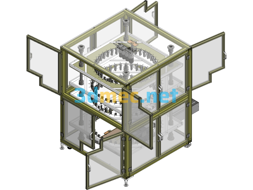
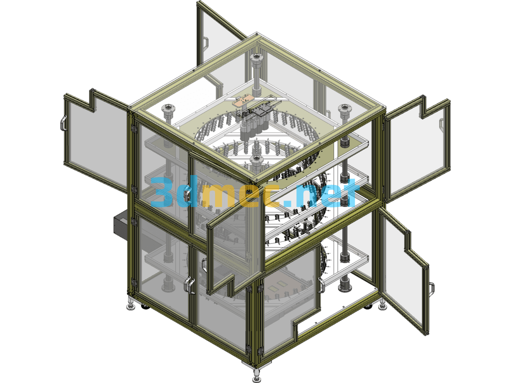
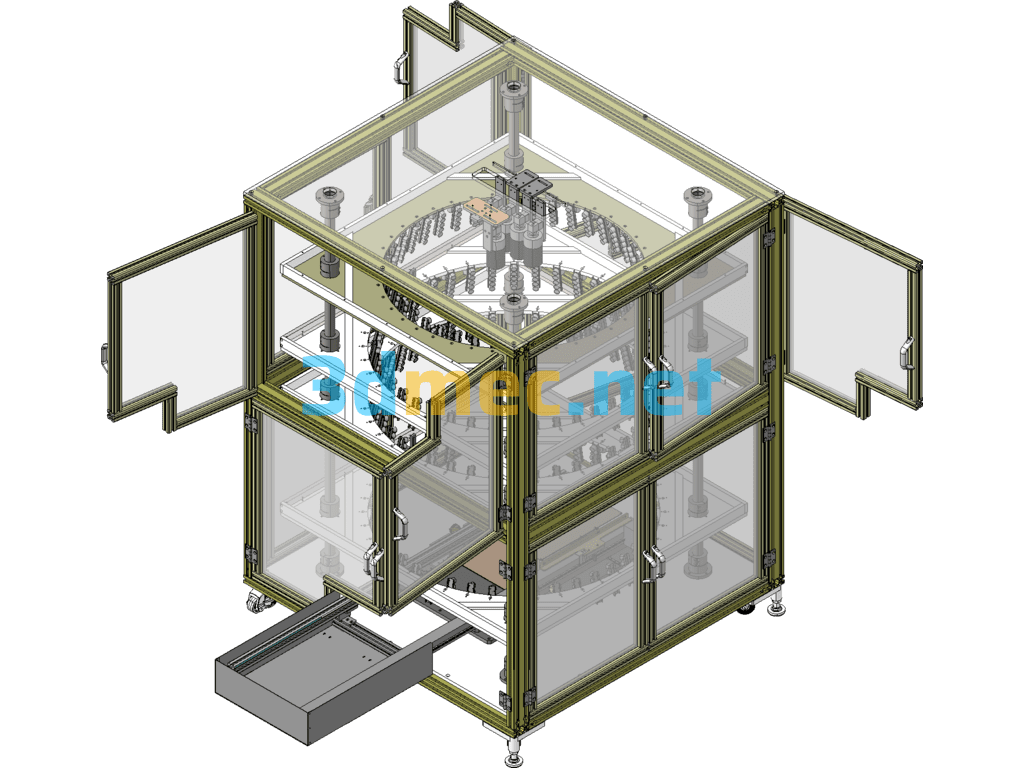
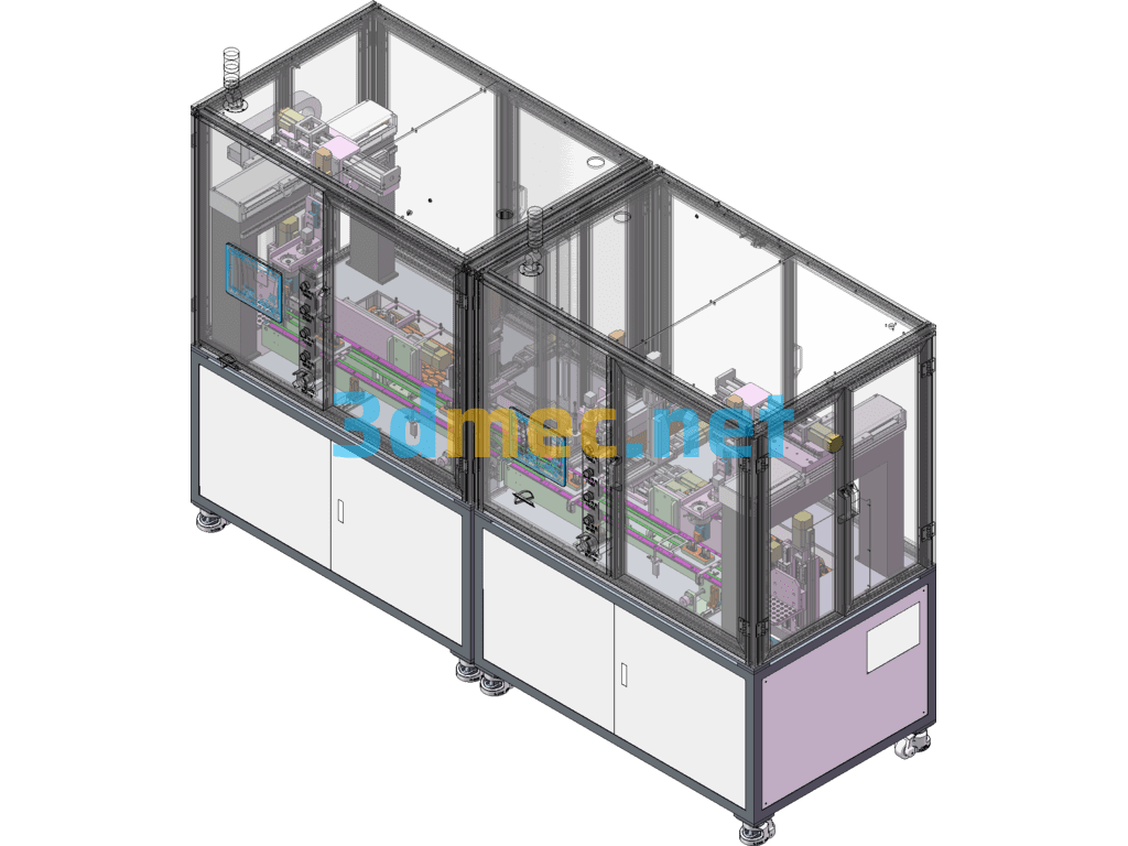
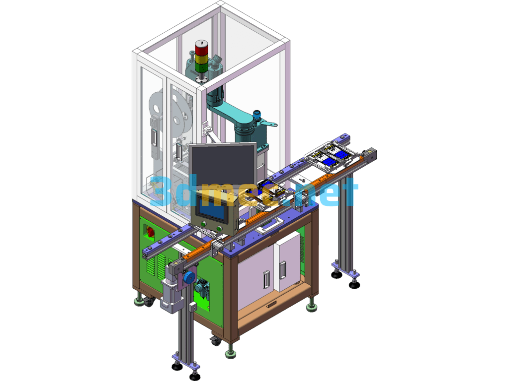
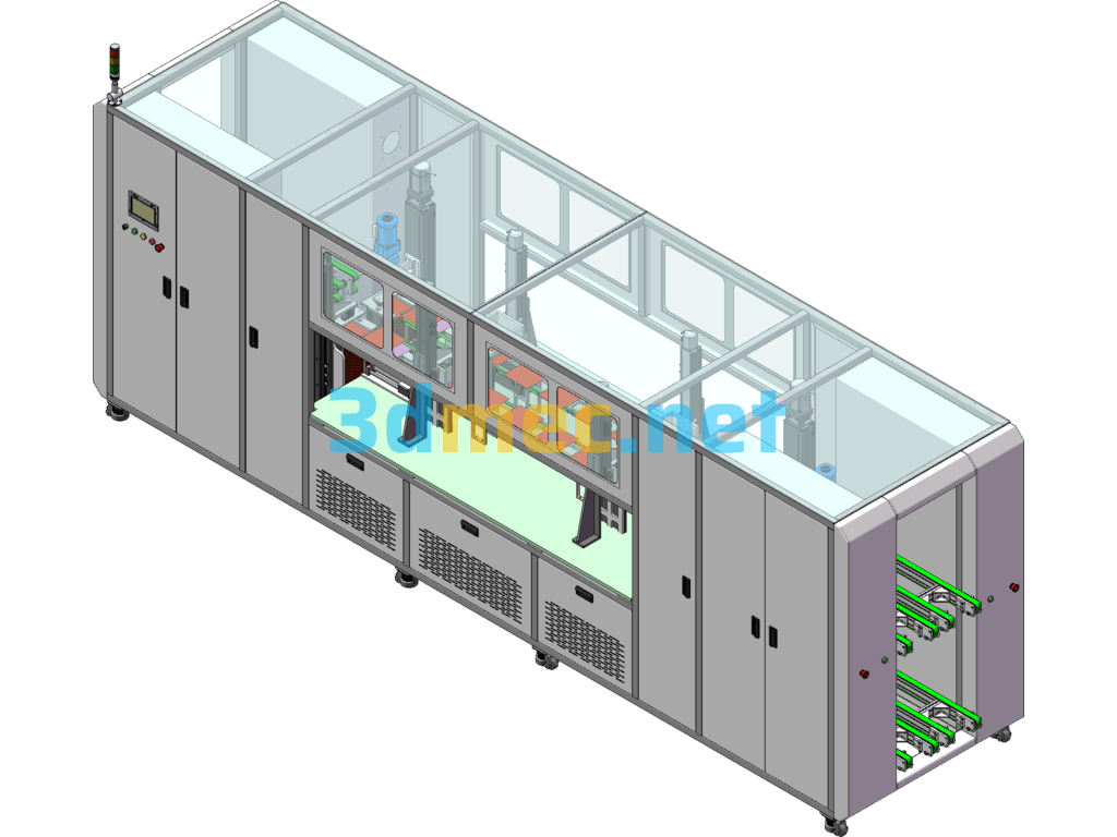
Large PCB tin spot visual inspection equipment 3D model SW2013 design Sldprt/Sldasm source file provides document with parameters and can be edited. For the inspection of large PCB boards, the visual CCD is used to sample the board surface once for comparison and analysis, saving time and eliminating the need for distributed sampling; the core part of this machine is the innovative design of the layout of the CCD light source, and this machine has been put into use.
Specification: Large PCB Board Tin Spot Visual Inspection Equipment – 3D Model SolidWorks
|
User Reviews
Be the first to review “Large PCB Board Tin Spot Visual Inspection Equipment – 3D Model SolidWorks”
You must be logged in to post a review.





There are no reviews yet.