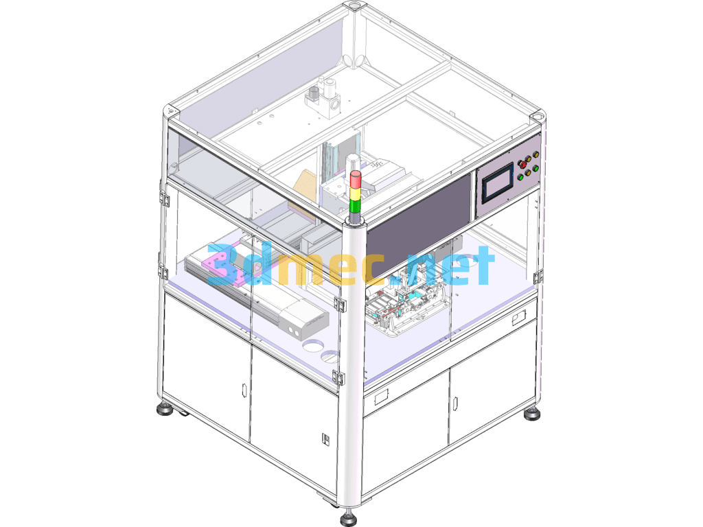
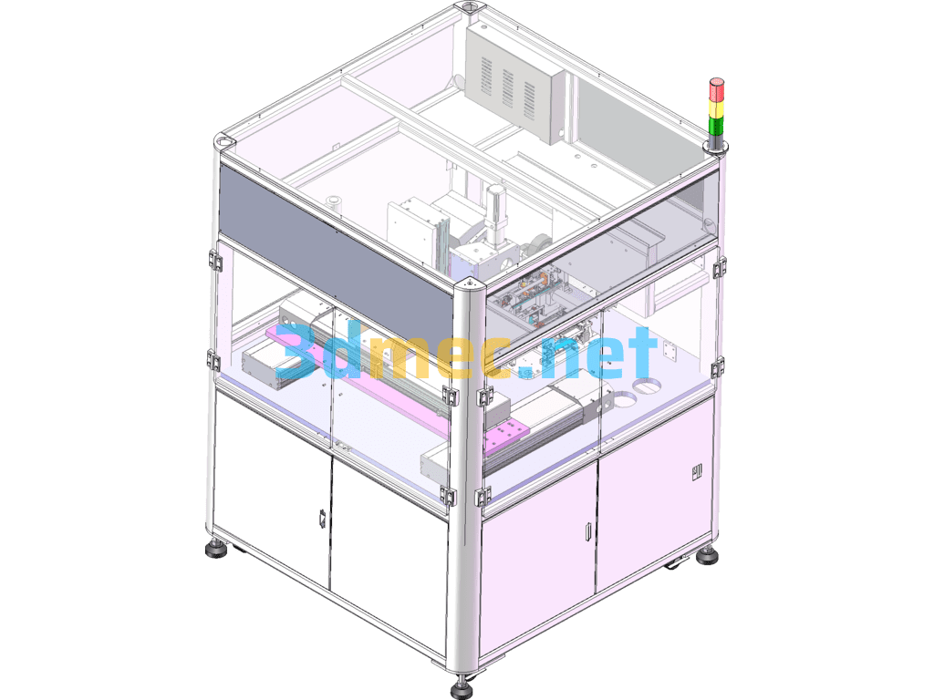
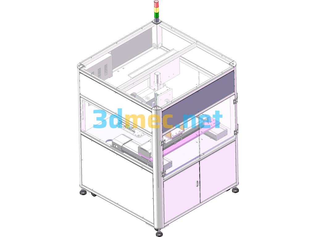
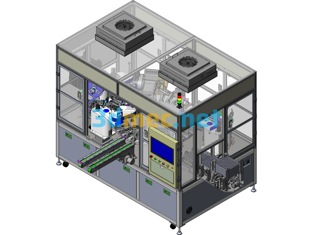
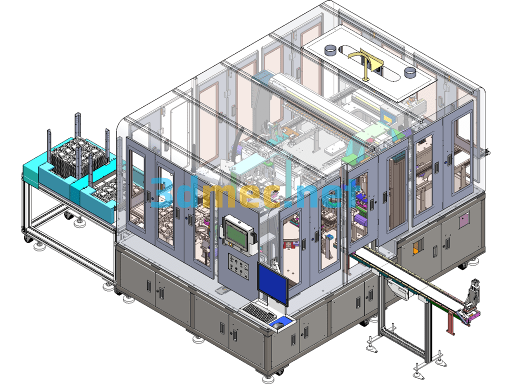
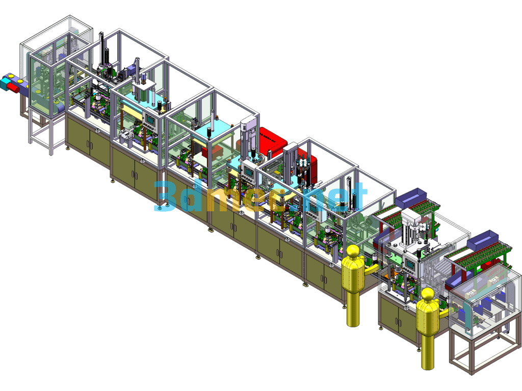
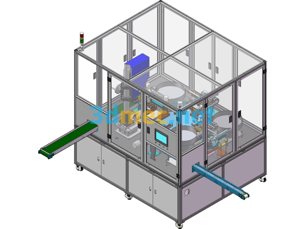
The mechanism of this equipment is designed by SW2016 and includes editable part features. It is suitable for chip component placement in the semiconductor integrated circuit production process (back-end packaging), realizing dispensing, dipping, chip bonding, chip bonding, wafer bonding, flip packaging, GaAs, and the chip bonding pressure is controllable with high precision. It adopts a precision magnetic suspension motion platform, and the main system X and Y axes use a contactless and frictionless magnetic suspension system with a high-resolution linear encoder. The encoder scale has an accuracy of 0.02μm, which can achieve high-speed, precise, sub-micron positioning. Rotation angle: The equipment has a 360-degree rotation function, and the rotation resolution accuracy is 0.01 degrees, which can realize chip placement at any angle during the assembly process. Contains STP and UG universal editable formats.
Specification: Automatic Patch Molding Equipment Semiconductor Integrated Circuit Back-End Packaging – 3D Model SolidWorks
|
User Reviews
Be the first to review “Automatic Patch Molding Equipment Semiconductor Integrated Circuit Back-End Packaging – 3D Model SolidWorks”
You must be logged in to post a review.



There are no reviews yet.